Beyond Silicon in 2026: How IMEC, TSMC, Intel, and Samsung Are Building Atomically-Thin 2D Transistors to Keep Moore’s Law Alive
- Internet Pros Team
- July 19, 2026
- AI & Technology
Every phone, laptop, and AI data center runs on the same quiet miracle: a transistor, a tiny switch that has been shrinking for sixty years. Silicon made it possible, and shrinking it is what gave us cheaper, faster, more powerful computers decade after decade. But in 2026 that switch has been shrunk so far that silicon itself has become the problem - the channel it carries current through is now only a handful of atoms wide, and at that size silicon starts to leak, misbehave, and waste power. The industry’s answer is radical: stop making the channel out of silicon at all, and build it instead from 2D semiconductors - materials just one or a few atoms thick.
Why Silicon Ran Out of Room
A transistor is a switch with three parts: a channel that current flows through, and a gate that turns that flow on or off. For decades progress meant making the channel shorter so more transistors fit on a chip. But a shorter channel is harder for the gate to control. When the channel gets thick relative to its length, current sneaks through even when the switch is supposed to be off - a leak that wastes power and generates heat. To keep control, engineers have to make the channel not just shorter but thinner. Silicon can only be thinned so far before its surface atoms start scattering electrons and its electrical behavior falls apart, usually around a few nanometers. That is the wall the whole industry hit.
"We are no longer shrinking the transistor - we are re-inventing the material it is made of. The next decade of computing belongs to whoever can grow a perfect crystal one atom thick, at wafer scale, every single time."
What Makes a 2D Semiconductor Different
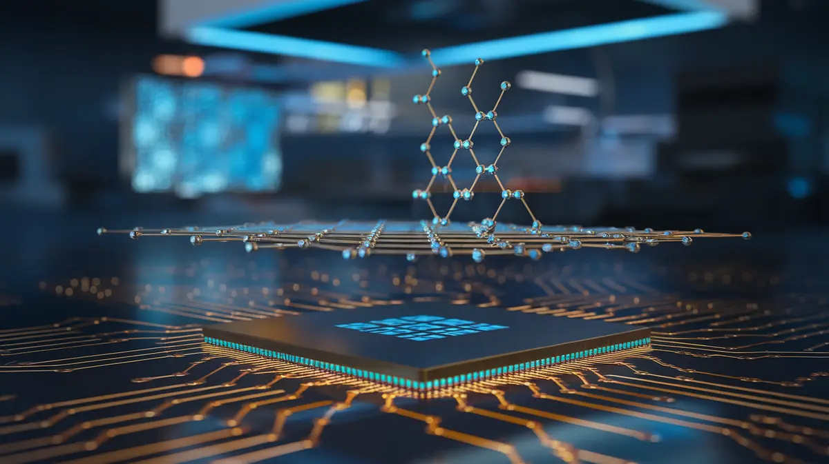
A 2D semiconductor is a material that stays a good semiconductor even when it is only one molecule thick - a flat sheet where every atom is on the surface and there is no bulk underneath. The leading family is called transition metal dichalcogenides, or TMDs, and the poster child is molybdenum disulfide (MoS2): a single layer of molybdenum atoms sandwiched between two layers of sulfur, less than a nanometer tall. Because it is already atomically thin, a 2D channel gives the gate near-total control over the current, so the switch turns off cleanly with almost no leak - exactly the behavior silicon loses at the same size.
This is why people say the industry has entered the angstrom era: the meaningful dimension is no longer counted in nanometers but in angstroms, tenths of a nanometer - the thickness of individual atoms.
The Four Hard Problems Standing in the Way
2D transistors work beautifully in the lab. Turning them into billions of identical switches on a 300 mm wafer is where the real fight is, and it comes down to four problems.
1. Growing a Perfect Sheet
A monolayer has to be grown flawlessly across an entire wafer with no gaps or grain boundaries. Flaking crystals off by hand made great physics papers; wafer-scale, defect-free growth is the manufacturing prize of 2026.
2. Making Good Contacts
Getting current in and out of a sheet one atom thick is brutally hard. A bad metal contact adds resistance that erases the speed advantage, so low-resistance contacts are a field of research all their own.
3. Doping Without Bulk
Silicon is tuned by implanting impurity atoms into its bulk. A 2D sheet has no bulk to implant into, so engineers must dope the surface with new tricks that do not tear the crystal apart.
4. Low-Temperature Integration
To stack 2D layers on top of finished silicon, they must be grown or transferred at low temperature so the circuits below survive - the key to 3D-stacked, CFET-style chips.
Who Is Building It
This is not a science-fiction bet - the largest names in chips have put 2D materials directly on their public roadmaps.
- IMEC - the Belgian research hub that the whole industry leans on has become the center of gravity for 2D transistors, demonstrating wafer-scale MoS2 devices and mapping out how a 2D channel slots into future gate-all-around and CFET architectures.
- TSMC - the world’s largest foundry has published sustained research on 2D-material transistors and low-resistance contacts, treating them as a candidate channel for nodes beyond what silicon can reach.
- Intel - its components-research team has shown gate-all-around devices built with 2D channels and has openly targeted stacking 2D transistors to keep doubling density into the next decade.
- Samsung - already shipping gate-all-around silicon at the leading edge, it is investing heavily in 2D materials and even alternative uses like ultra-thin memory as the successor material.
- University and national labs - MIT, Stanford, and teams across Asia and Europe keep pushing new TMDs, better growth recipes, and the contact and doping chemistry the foundries need.
Silicon vs 2D: A Handoff, Not a Coup
It is tempting to frame this as 2D killing silicon. The reality is a slow handoff, one layer at a time.
| Dimension | Silicon Channel | 2D Semiconductor Channel |
|---|---|---|
| Thinnest usable channel | A few nanometers before it breaks down | Under 1 nm - a single molecule |
| Gate control at tiny sizes | Leaks and wastes power | Switches off cleanly |
| Manufacturing maturity | Sixty years, extremely refined | Early, wafer-scale growth still hardening |
| Best near-term role | Today’s and tomorrow’s mainstream chips | The topmost, most-scaled logic layers |
The Honest Trade-Offs
2D transistors are not a free win. Yield is the giant hurdle: a process that makes a perfect device one time in ten is a triumph in a lab and a catastrophe in a fab that needs billions of identical switches. Contact resistance still eats into the theoretical speed gains. The materials and tooling are new, so cost is high and supply chains are thin. And silicon is a moving target - gate-all-around nanosheets and backside power delivery are squeezing more life out of it, buying the industry time and raising the bar 2D has to clear.
Why This Matters for Business
You will never buy a molybdenum disulfide transistor, but you will feel it. The entire modern economy - and especially the AI boom - runs on the assumption that computing keeps getting cheaper and denser. That assumption is exactly what silicon scaling can no longer guarantee on its own. 2D semiconductors are one of the few credible paths to keeping the cost-per-transistor curve bending downward, which is what lets the next generation of AI models, edge devices, and data centers stay affordable to run.
For technology leaders, the takeaway is not to track angstroms - it is to understand that the ground floor of computing is being rebuilt, and that the timeline of ever-cheaper compute your plans depend on now hinges on exotic materials science moving from the lab to the fab. The companies that grasp early where compute costs are heading - and design their products, pricing, and AI strategy around it - will have a real edge over those who assume the old curve continues on autopilot.
"Silicon got us here. It will not get us to the end of the decade alone. The first company to ship a reliable 2D transistor at scale will quietly reset the economics of computing for everyone else."
The transistor has been shrinking since before most of us were born, and it was easy to assume it always would. In 2026 that shrinking finally required changing what the switch is made of. Whether the future is molybdenum disulfide, tungsten diselenide, or something not yet named, the message is the same: the age of silicon-only computing is ending, and the atomically thin era has begun.