Chiplet Architecture in 2026: How Modular Silicon Is Reshaping CPUs, GPUs, and AI Accelerators
- Internet Pros Team
- April 20, 2026
- AI & Technology
In March 2026, NVIDIA shipped its Blackwell Ultra GB300 AI accelerator — a single package containing two reticle-sized GPU dies, eight stacks of HBM3e memory, and a network of silicon bridges stitching everything together into what the chip industry calls one "super-chip." A month earlier, AMD's MI400 shipped with twelve chiplets on a single substrate. Apple's M4 Ultra glued two M4 Max dies together with a 10-terabit-per-second interconnect. Intel's Clearwater Forest Xeon packed 288 efficiency cores across seven tiles. The pattern is unmistakable: the monolithic chip — a single slab of silicon doing everything — is finished as the dominant paradigm for high-performance computing. In its place is the chiplet: small, specialized silicon dies, each manufactured on the process node that best fits its function, then assembled into a package that behaves like one enormous processor. 2026 is the year this architecture became the default across every serious CPU, GPU, and AI accelerator shipping at scale.
What Is a Chiplet?
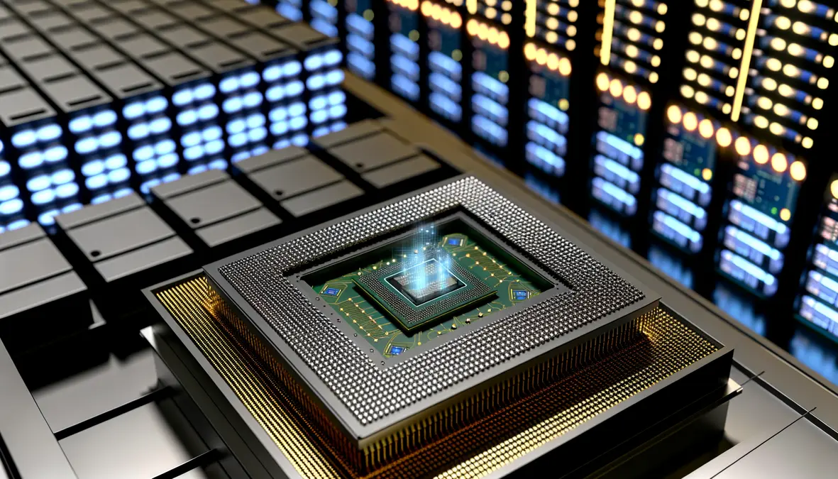
A chiplet is a discrete silicon die designed to be combined with other dies on a single package through high-speed interconnects and advanced packaging. Instead of fabricating one giant monolithic chip with CPU cores, cache, memory controllers, I/O, and accelerators all on the same piece of silicon, a chiplet-based design breaks those functions into separate dies — often on different process nodes — and links them together using silicon interposers, embedded bridges, or organic substrates. To the software and to the rest of the system, the finished package still looks like a single processor, but underneath it is a heterogeneous mini-network of specialized silicon.
The approach trades one problem (designing and yielding a giant reticle-limited die) for a different set of problems (packaging complexity, die-to-die bandwidth, thermal management) — and in 2026 those tradeoffs overwhelmingly favor chiplets for anything large, expensive, or performance-critical.
Better Yields, Lower Cost
Small dies have dramatically higher wafer yields than reticle-sized monoliths. A defect in one chiplet discards a postage-stamp of silicon, not a $20,000 processor.
Mix & Match Process Nodes
Put compute on leading-edge 2nm, I/O and cache on mature 6nm, analog on 16nm. Each function is built where the economics make sense, not forced onto one node.
Escape the Reticle Limit
Lithography reticles cap a monolithic die at ~858 mm². Chiplets compose multiple dies into packages 2–4× larger, unlocking more cores, more cache, more AI performance.
Why the Monolithic Era Is Ending
For thirty years, Moore's Law made the monolithic chip a good bet: shrink the process, cram more transistors onto one die, and the economics worked. That deal has broken down. Leading-edge 3nm and 2nm wafers now cost $20,000 or more, and defect density on early nodes is brutal. A single large die at 600 mm² may yield fewer than 30% good chips off a wafer, while a 100 mm² chiplet on the same process yields over 85%. When yields are that different, the cost-per-transistor math flips hard in favor of smaller dies.
AI workloads have made the situation even more urgent. Training and serving frontier models demands package-level bandwidth and memory capacity that no single reticle-limited die can provide. NVIDIA's Blackwell generation solved this by bonding two near-reticle dies together with an NV-HBI interconnect and treating the pair as one logical GPU. AMD's MI300X connects eight compute chiplets to four I/O dies stacked on top of a base interposer. Neither design is possible as a monolith — the reticle limit physically forbids it.
| Dimension | Monolithic Chip | Chiplet-Based Design |
|---|---|---|
| Max Die Size | ~858 mm² (reticle limit) | 3,000+ mm² per package |
| Process Node | One node for the whole chip | Mix leading-edge + mature nodes |
| Yield at 2nm/3nm | 30–50% for large dies | 80–90% for small dies |
| Design Reuse | Redesign per product | Compose products from die library |
| Time to Market | Slow — tape out the whole SoC | Faster — assemble proven tiles |
| Best For | Cost-sensitive mobile & embedded | Servers, AI accelerators, high-end client |
Who's Shipping Chiplets in 2026
Every major chip vendor has bet the next generation of flagship products on chiplet architecture. The designs differ in how aggressively they decompose the SoC and what packaging technology they use, but the direction is universal.
- AMD Instinct MI300 / MI400: The reference AI accelerator for chiplet maximalism. MI300X uses 8 XCD compute chiplets, 4 IOD I/O dies, and 8 HBM3 stacks on a single package via 3D hybrid bonding and CoWoS-S packaging. MI400, shipping in 2026, pushes core count higher and adds optical I/O chiplets.
- AMD EPYC & Ryzen: Zen 5 server CPUs ship with up to 16 CCD compute chiplets on 3nm plus a single I/O die on 6nm, all stitched by Infinity Fabric. The architecture let AMD reach 192 cores per socket while competitors were still yield-limited at 64.
- NVIDIA Blackwell & Blackwell Ultra: GB200 and GB300 pair two massive GPU dies over a 10 TB/s NV-HBI link. Rubin, NVIDIA's next platform, extends the approach to four dies and adds disaggregated memory chiplets.
- Intel Meteor Lake, Lunar Lake, Clearwater Forest: Intel's tile strategy uses Foveros 3D and EMIB 2.5D packaging to combine compute, graphics, I/O, and NPU tiles fabricated on different nodes — often mixing Intel's own fabs with TSMC-sourced tiles.
- Apple M4 Ultra: Two M4 Max dies bonded with a 10 Tbps UltraFusion interconnect, presented to software as one 32-core processor with unified memory — a chiplet in everything but marketing copy.
- Tesla Dojo D2, Cerebras, and Groq: AI-specific silicon vendors using chiplet decomposition to scale wafer-scale and multi-die training accelerators beyond what monolithic designs can physically support.
"The reticle limit is the end of the road for monolithic scaling. Chiplets are not a clever optimization — they are the only way forward for anything that needs more compute than a single lithography mask can print."
UCIe: The Standard That Made Chiplets an Ecosystem
The biggest structural change in 2025-2026 was the maturation of UCIe (Universal Chiplet Interconnect Express), an open die-to-die interconnect standard backed by AMD, Intel, ARM, TSMC, Samsung, Qualcomm, Google, Microsoft, Meta, and dozens of smaller vendors. UCIe defines both the physical layer (pin pitch, signaling, power delivery) and the protocol layer (PCIe and CXL semantics for chiplets), so a compute tile from one vendor can be combined with an I/O tile or accelerator tile from another.
UCIe 2.0, ratified in 2024 and widely implemented in 2026, added 3D stacking support, per-lane speeds up to 32 GT/s, and the management-layer primitives needed for reliability, availability, and serviceability in production systems. UCIe 3.0, due in 2027, targets 64 GT/s and formalizes optical chiplet integration. The practical consequence is an emerging chiplet marketplace: specialized IP vendors can ship silicon tiles (not just Verilog) and system integrators can shop for compute, memory, I/O, and accelerator dies the way they shop for PCIe cards today.
Advanced Packaging: The Real Enabler
Chiplets only work because advanced packaging got dramatically better. Three technology families now dominate production in 2026:
- Silicon interposers (2.5D): A passive silicon substrate with fine-pitch wiring that connects chiplets side by side. TSMC's CoWoS (Chip-on-Wafer-on-Substrate) is the most widely used variant and underpins nearly every high-end AI accelerator shipping today, including Blackwell and MI300.
- Embedded silicon bridges: Intel's EMIB places small silicon bridges inside an organic substrate only where two chiplets meet. It avoids the cost of a full interposer while retaining most of the bandwidth benefits — a pragmatic middle ground used across Intel's client and server tiles.
- 3D hybrid bonding: Face-to-face bonding of dies using copper-to-copper connections at sub-micron pitch. Intel's Foveros, AMD's 3D V-Cache, and TSMC's SoIC enable vertical integration: cache stacked on logic, memory stacked on compute, with thousands of connections per square millimeter.
Capacity for advanced packaging is now the scarcest resource in the semiconductor supply chain. TSMC CoWoS output is sold out through 2027, and the NVIDIA-AMD-Broadcom scramble for packaging slots has become as strategic as the fight for leading-edge wafers themselves.
Challenges That Keep Chiplets From Being Free
The decomposition is not a silver bullet. Several engineering problems get harder, not easier, when you split a chip apart:
- Die-to-die bandwidth and latency: Crossing a package boundary costs power and picoseconds. Workloads with irregular memory access patterns can lose more from the inter-chiplet hop than they gain from extra cores.
- Thermal density: Stacking chiplets vertically concentrates heat. 3D designs demand new cooling strategies — micro-fluidic channels, direct-die liquid, advanced thermal interface materials.
- Known-good-die testing: A single bad chiplet ruins a multi-die package. Testing dies before packaging — at sub-micron bond pad pitch — is now a first-order production problem.
- Software and scheduling: NUMA effects across chiplets require operating systems, runtimes, and AI frameworks to understand package topology. PyTorch, JAX, and CUDA all expose topology-aware primitives in 2026 that did not exist two years ago.
What This Means for Your Business
For most software teams, chiplets are a hardware detail that the toolchain absorbs. But the architecture shift has real consequences worth planning around. Cloud instance types are becoming more heterogeneous and more topology-aware — the performance of AI training and HPC workloads increasingly depends on how well the scheduler respects chiplet boundaries, NUMA domains, and memory locality. Teams that profile their workloads against concrete instances, rather than trusting generic "vCPU" counts, will continue to see outsized gains.
For hardware-adjacent businesses — robotics, edge AI, networking, industrial IoT — the chiplet marketplace enabled by UCIe opens a door that used to be shut to anyone without a billion-dollar SoC budget. Small teams can now license or buy proven compute and I/O tiles and focus their own silicon effort on the differentiating accelerator, dropping time-to-silicon from five years to eighteen months for focused designs.
Key Takeaways for 2026
- Monolithic is over at the high end: Every flagship CPU, GPU, and AI accelerator in 2026 is a chiplet design. The reticle limit and 2nm yields make anything else uneconomic.
- UCIe is the new PCIe: A standard die-to-die interconnect backed by the whole industry is turning chiplets from a per-vendor trick into an open ecosystem.
- Packaging is the new bottleneck: TSMC CoWoS, Intel Foveros, and 3D hybrid bonding capacity is more constrained than leading-edge wafer supply — and more strategically valuable.
- Software must get topology-aware: Runtimes, schedulers, and AI frameworks that respect chiplet boundaries outperform those that treat a package as one flat processor.
- Smaller silicon teams become viable: Standard chiplets plus custom accelerator tiles drop the cost and time of getting differentiated silicon to market.
For half a century the chip industry treated the monolithic die as a default: make it bigger, shrink the transistors, keep going. That model gave us the modern world, and now it is retiring into a narrower role. The machines training tomorrow's frontier models and running tomorrow's cloud are already packages of specialized silicon — tile libraries assembled into processors that no single die could ever be. In 2026, the chip is no longer a chip. It is a stack, a mosaic, a system in a package. And the products built on top of that idea are quietly redefining what computing looks like at every level above them.