Photonic Computing: How Light-Based Processors Are Revolutionizing AI and Data Centers in 2026
- Internet Pros Team
- March 20, 2026
- AI & Technology
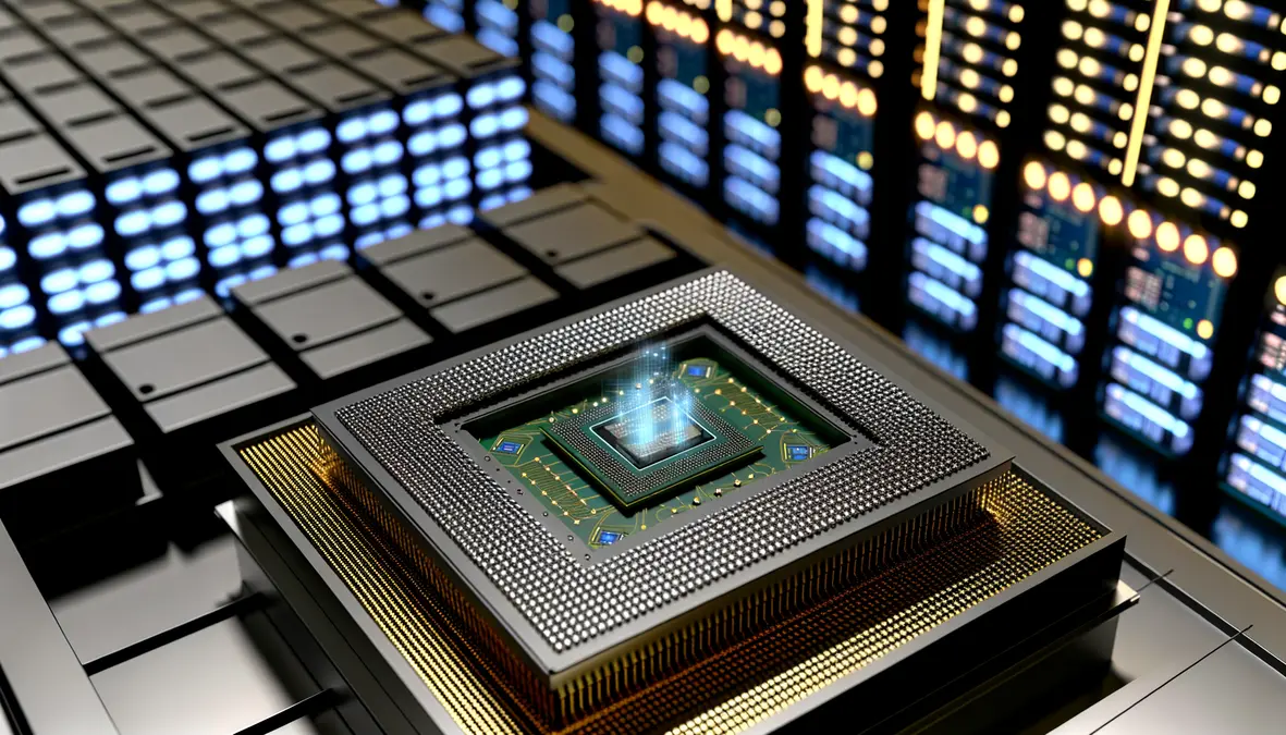
In February 2026, Lightmatter announced that its Passage photonic interconnect fabric had been deployed in a hyperscale data center operated by one of the world's largest cloud providers, connecting 16,384 AI accelerator chips with optical signals traveling at the speed of light — replacing copper cables that had become the single biggest bottleneck in AI training clusters. The result: a 4.2x improvement in chip-to-chip communication bandwidth with 93 percent less energy consumed by the interconnect layer. Across the industry, photonic computing — the use of photons (particles of light) instead of electrons to process, transmit, and store data — has crossed a critical inflection point. After decades of academic research and false starts, breakthroughs in silicon photonics, photonic integrated circuits (PICs), and optical AI accelerators are delivering real-world performance gains that electronic processors alone can no longer achieve, positioning light-based computing as the defining hardware revolution of the AI era.
Why Photons Are Replacing Electrons
The fundamental physics of light give photonic computing three decisive advantages over traditional electronic processors. First, photons travel at the speed of light — approximately 300,000 kilometers per second — and can carry data across optical fibers and waveguides with virtually zero signal degradation and no electromagnetic interference. Second, multiple wavelengths of light can travel through the same optical fiber simultaneously using wavelength-division multiplexing (WDM), enabling a single fiber to carry terabits of data per second — orders of magnitude more than a copper wire of equivalent size. Third, and most critically for the AI era, photons generate almost no heat during transmission, addressing the single biggest constraint facing the semiconductor industry: power consumption and thermal management.
| Property | Electronic Computing | Photonic Computing | Advantage |
|---|---|---|---|
| Signal Speed | ~70% speed of light in copper | Speed of light in optical media | ~30% faster signal propagation |
| Bandwidth Density | Limited by wire count and frequency | Wavelength-division multiplexing (100+ channels) | 100x+ bandwidth per link |
| Energy per Bit | ~5-10 picojoules per bit (interconnect) | ~0.1-0.5 picojoules per bit | 10-50x more energy efficient |
| Heat Generation | Significant (requires active cooling) | Minimal during transmission | Dramatically reduced cooling costs |
| Matrix Multiplication | Sequential clock cycles (O(n²)) | Single pass through optical mesh (O(1)) | Orders of magnitude faster for AI inference |
The energy advantage alone is transformative. With AI data centers projected to consume 4.5 percent of global electricity by 2027, photonic computing offers a path to continue scaling AI model size and training without proportionally scaling energy consumption. NVIDIA CEO Jensen Huang acknowledged this shift at GTC 2026, stating that optical interconnects would become "essential infrastructure" for next-generation GPU clusters, and announcing a partnership with Ayar Labs to integrate optical I/O chiplets into future Blackwell GPU architectures.
"The AI industry has hit an energy wall. We cannot keep doubling the size of training clusters while doubling their power consumption. Photonics is not optional — it is the only path to sustainable AI scaling. Light does what electrons physically cannot: move massive amounts of data with almost zero energy cost."
Silicon Photonics: Manufacturing Light on Chip
The key enabler of the photonic computing revolution is silicon photonics — the fabrication of optical components (waveguides, modulators, detectors, and multiplexers) directly on standard silicon wafers using existing CMOS semiconductor manufacturing processes. This means photonic chips can be produced in the same foundries that manufacture electronic processors, leveraging decades of semiconductor manufacturing expertise, existing supply chains, and economies of scale. GlobalFoundries, TSMC, and Intel Foundry Services all offer silicon photonics process design kits (PDKs), and production volumes have increased 300 percent between 2024 and 2026.
Photonic Integrated Circuits (PICs)
PICs integrate hundreds of optical components — lasers, modulators, waveguides, filters, and photodetectors — onto a single chip smaller than a fingernail. Companies like Infinera, Intel, and Broadcom are shipping PICs with over 1,600 optical components per chip, enabling 800G and 1.6T optical transceivers that form the backbone of hyperscale data center networks. The integration density of PICs is doubling approximately every 18 months, following an optical equivalent of Moore's Law.
Co-Packaged Optics (CPO)
CPO places photonic chiplets directly alongside electronic processors on the same package substrate, eliminating the energy-hungry electrical traces between the processor and pluggable optical modules. Broadcom's Bailly CPO platform and Marvell's co-packaged optical solutions reduce interconnect power by up to 70 percent while increasing bandwidth density. CPO is expected to become the standard architecture for AI accelerator packaging by 2028.
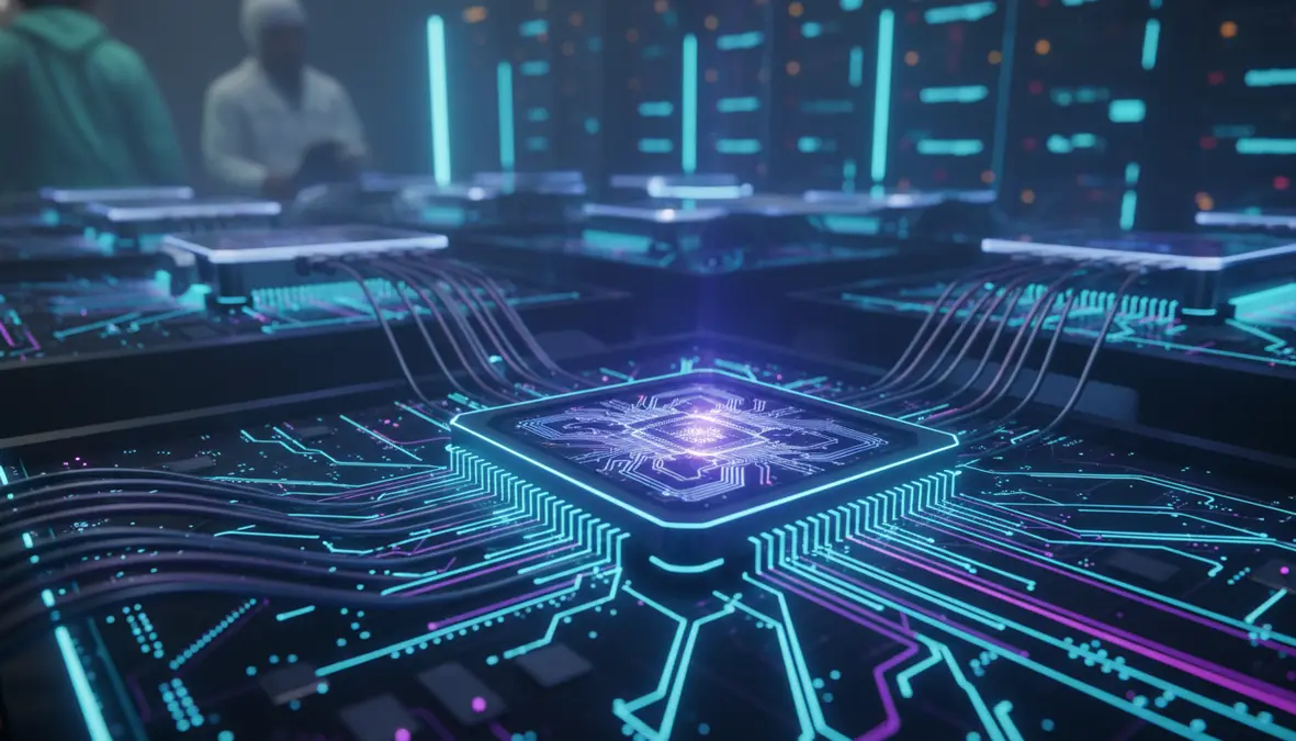
Optical AI Accelerators: Computing with Light
Perhaps the most revolutionary application of photonic computing is using light itself for computation — not just data transmission. Optical neural network accelerators perform the matrix multiplications at the heart of AI inference by passing light through carefully configured arrays of optical components (Mach-Zehnder interferometers, phase shifters, and microring resonators) that multiply input vectors by weight matrices in a single pass at the speed of light, consuming a fraction of the energy required by electronic GPU or TPU operations.
Lightmatter Envise
Lightmatter's Envise photonic AI accelerator uses programmable photonic meshes to perform matrix-vector multiplications optically. Benchmarks show 10x better energy efficiency than leading electronic accelerators for transformer inference workloads, with sub-microsecond latency for large matrix operations.
Lightelligence Hummingbird
Lightelligence's Hummingbird optical AI chip integrates over 16,000 photonic components on a single die, targeting recommendation systems and natural language processing. The chip performs 1,000 trillion operations per second per watt — roughly 100x the efficiency of current GPUs for specific AI workloads.
Xanadu Aurora
Xanadu's Aurora photonic quantum-classical hybrid processor combines photonic qubits with classical photonic computing for optimization problems. Aurora represents the convergence of photonic computing and quantum computing — two light-based paradigms that may ultimately merge into a unified optical computing architecture.
Photonic Interconnects: Solving the AI Bandwidth Crisis
While optical computation is still emerging, photonic interconnects have already become mission-critical infrastructure in AI data centers. Training frontier AI models like GPT-5 and Gemini Ultra requires thousands of GPUs to communicate massive volumes of gradient data during distributed training. With electronic interconnects, up to 40 percent of total training time is spent waiting for data to move between chips — a bottleneck that photonic interconnects directly eliminate.
- Lightmatter Passage: A wafer-scale photonic interconnect fabric that connects up to 48 chips in an all-to-all topology using optical waveguides fabricated directly on a silicon interposer. Passage eliminates the need for electronic switches between chips, reducing latency by 10x and power consumption by 93 percent compared to equivalent electronic mesh networks
- Ayar Labs TeraPHY: An optical I/O chiplet that replaces electrical SerDes with optical transceivers, delivering 2 terabits per second of bandwidth in a package that consumes less than 5 picojoules per bit. NVIDIA, Intel, and HPE have all announced integration plans for Ayar Labs optical I/O technology
- Cisco Silicon One with Photonics: Cisco's latest networking ASICs integrate co-packaged optics to deliver 51.2 terabits per second of switching capacity for AI data center fabrics, enabling non-blocking communication between thousands of AI accelerators
- Broadcom Tomahawk 6: Broadcom's next-generation switch chip pairs 102.4 Tbps switching capacity with CPO interfaces, targeting the AI cluster networking market where bandwidth demand is growing 2x annually
The Road Ahead: Challenges and Opportunities
Despite rapid progress, photonic computing faces significant challenges. Optical components are inherently analog, requiring precise calibration and temperature control that complicates manufacturing at scale. Photonic AI accelerators currently excel at linear algebra operations (matrix multiplications) but require electronic components for nonlinear activation functions, memory access, and control logic — making today's photonic processors hybrid optical-electronic systems rather than pure optical computers. Additionally, the photonic computing ecosystem — design tools, programming frameworks, and developer expertise — is still immature compared to the decades-old electronic computing ecosystem dominated by CUDA, PyTorch, and x86 architectures.
However, the trajectory is clear. The global silicon photonics market is projected to reach 7.8 billion dollars by 2028, growing at a compound annual rate of 25.3 percent. Every major cloud provider — Amazon, Google, Microsoft, Meta, and Oracle — has active photonic computing programs. TSMC has announced a dedicated silicon photonics process node optimized for co-packaged optics, and NVIDIA's roadmap shows optical interconnects becoming standard in GPU clusters by 2027. The convergence of AI's insatiable demand for compute, the physical limits of electronic scaling, and the maturation of silicon photonics manufacturing is creating the conditions for photonic computing to become not just a niche technology but a foundational pillar of the computing industry.
What This Means for Your Business
The photonic computing revolution will impact businesses across the technology stack. Organizations running large-scale AI workloads should evaluate photonic interconnect solutions that can dramatically reduce training costs and energy consumption. Data center operators should plan for co-packaged optics and optical switching in their next-generation network architectures. Telecom providers are already deploying coherent optical systems with silicon photonic transceivers to meet 5G and 6G backhaul demands. And software developers building AI applications should monitor photonic AI accelerator platforms, as new programming models and APIs emerge that expose optical computing capabilities to application code.
At Internet Pros, we help businesses navigate the rapidly evolving computing landscape — from evaluating next-generation infrastructure technologies to building applications that leverage cutting-edge hardware capabilities. Whether you need guidance on data center architecture, AI infrastructure planning, or technology strategy, our team stays at the forefront of innovations like photonic computing to ensure your business is prepared for the future. Contact us today to discuss how emerging computing technologies can give your organization a competitive edge.