Backside Power Delivery (BSPDN): How PowerVia, Super Power Rail, and Buried Power Rails Are Rewiring the Chip Stack to Unlock 2nm and Beyond in 2026
- Internet Pros Team
- May 16, 2026
- AI & Technology
For sixty years, every transistor on a silicon chip drew its power from above. Tens of metal layers stacked on top of the wafer carried both the signals that did the computing and the power that fed the computing — and as transistors shrank, the two functions began to physically fight for the same wires. In 2026, that war is finally being settled by flipping the chip upside down. Backside Power Delivery Networks (BSPDN) — shipping today as Intel PowerVia on the Intel 18A node, and arriving this year as TSMC Super Power Rail on N2P and Samsung BSPDN on SF2 — move every power wire to the underside of the silicon wafer. The front side is freed to do nothing but route signals. The result is the single biggest interconnect reorganization since the introduction of copper damascene in the 1990s, and it is the lever that finally unlocks the 2nm and Angstrom-era process nodes that will power NVIDIA Rubin Ultra, AMD MI500, AWS Trainium 4, Apple M5, and Google TPU v8.
Why Front-Side Power Hit Its Wall
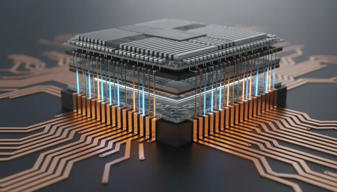
A modern chip has 15 to 20 layers of copper interconnect sitting on top of the transistors. Historically, the lowest few layers — the so-called M0–M2 metals — carry the most critical signal routes between gates, while higher layers carry both wider signal buses and the chunky power rails (VDD and VSS) that feed current down to the cells. As gate pitches dropped below 50 nanometers, this stack became impossibly congested. Power wires need wide, low-resistance metal; signal wires need many narrow tracks at minimum pitch. Forcing them to share the same back-end-of-line (BEOL) stack created severe IR drop (voltage sag under heavy load), routing congestion that forced larger standard cells, and a leakage cliff that made each new node less efficient than its predecessor predicted.
BSPDN solves the conflict architecturally rather than chemically. After the front side is finished, the wafer is bonded to a carrier wafer and thinned from the back to a few microns. A second metal stack — wide, low-resistance, dedicated entirely to power — is then built on the underside of the silicon. Tiny vertical vias called nano-TSVs punch through the substrate to deliver current directly into the source/drain contacts of each transistor cell.
"We used to spend half a design cycle arguing about which signals had to give way to a wider power rail. With PowerVia, that argument simply does not exist. Every signal track is a signal track. Every backside track is a power track. The chip plans itself."
What Actually Changes When You Move Power to the Backside
The physical reorganization is dramatic, but the engineering payoff lands across four distinct dimensions.
~4x Lower IR Drop
Backside power wires can be 5-10x wider than front-side equivalents because they no longer share track budget with signals. Intel measures roughly 4x reduction in voltage droop on PowerVia 18A versus an equivalent front-side design — directly enabling higher sustained clock frequencies under AI workloads.
5-10% Density Uplift
Removing power rails from the front side frees signal tracks inside every standard cell, shrinking effective cell area without changing transistor pitch. The downstream result is a denser library at the same node, on top of whatever GAA scaling the node already delivers.
Cleaner Signal Routing
Front-side BEOL becomes a dedicated signal fabric, dramatically reducing the routing congestion that has limited high-performance core layout since 7nm. Place-and-route tools converge faster, designers reach target frequencies earlier, and timing closure is less painful for AI accelerator macros.
Improved Thermals
Backside power lets the hottest transistor regions sit closer to the wafer surface that ultimately mates to the heat spreader. Combined with backside decoupling capacitors and silicon thinning, BSPDN-built chips run measurably cooler at the same workload, a big win for AI accelerators with 1,000-watt thermal envelopes.
Three Flavors, Three Roadmaps
| Foundry / Node | Backside Technology | 2026 Status |
|---|---|---|
| Intel 18A | PowerVia — the first commercial BSPDN, paired with RibbonFET GAA transistors | In high-volume production at Fab 52 (Arizona) and D1X (Oregon). Powering Panther Lake client SoCs, Clearwater Forest Xeons, and Intel Foundry external customers including Microsoft and the U.S. DoD RAMP-C program. |
| TSMC N2P / A16 | Super Power Rail (SPR) — a buried power rail variant landing on N2P in late 2026 and as the default on A16 | Risk production on N2P; A16 (1.6nm) with SPR enters volume in 2027. Expected sockets include NVIDIA Rubin Ultra, AMD MI500, Apple M5 Pro/Max, Qualcomm Snapdragon 8 Gen 5, and MediaTek Dimensity 9500. |
| Samsung SF2 / SF1.4 | Samsung BSPDN with MBCFET nanosheet GAA | Ramping at the Pyeongtaek S5 fab. Expected to anchor Samsung's own Exynos 2600, AWS Trainium 4 (rumored dual-foundry split), and a growing list of Samsung Foundry HPC customers seeking a non-TSMC alternative. |
| Rapidus 2nm (Japan) | BSPDN co-developed with IBM, targeting domestic Japanese AI silicon | Pilot line at the IIM-1 fab in Hokkaido. First customer tape-outs expected late 2026, with volume production in 2027 — a strategic pillar of Japan's sovereign semiconductor push. |
The Engineering Cost of Going Backside
BSPDN is not free. Bonding a 300mm wafer to a carrier, thinning it from 775 microns down to 3-5 microns without cracking, etching nano-TSVs with sub-100-nanometer alignment to the front-side transistors, and then depositing a complete backside metal stack adds 30-40 process steps and roughly 10-15% to wafer cost at the leading edge. Test and debug also get harder — engineers can no longer probe internal nodes from the front, and infrared backside imaging is rendered partly opaque by the new metal stack.
Design enablement is its own mountain. Synopsys, Cadence, and Siemens EDA have all spent two years rewriting place-and-route, parasitic extraction, IR-drop, and electromigration tools to handle a fundamentally two-sided wiring graph. Standard cell libraries had to be redesigned from scratch. Foundry PDKs at 18A and N2P are roughly 25 percent larger than their predecessors. The transition is, in effect, the largest physical-design reset since the move from aluminum to copper interconnect.
What BSPDN Means for AI Buyers in 2026
- AI accelerator clocks finally climb again. Higher sustained frequencies at lower IR drop translate directly into more useful FLOPS per watt for training and inference workloads on Rubin Ultra, MI500, and Trainium 4.
- Sovereign foundries become competitive. Intel 18A with PowerVia in Arizona, Samsung SF2 in Pyeongtaek, and Rapidus 2nm in Hokkaido give hyperscalers and governments real second-source options outside Taiwan for the first time in a decade.
- Chiplet stacks get denser. Cleaner front-side routing pairs naturally with face-to-face hybrid bonding on the back, enabling tighter 3D IC integration with HBM and compute chiplets — the architecture behind every flagship 2026 AI socket.
- Mobile efficiency leaps. Apple M5, Qualcomm Snapdragon 8 Gen 5, and MediaTek Dimensity 9500 on N2P with SPR are projected to deliver 25-30 percent lower power at iso-frequency versus their N3P-class predecessors — a step-function gain for on-device AI inference.
- Supply, not silicon, is again the gating constraint. Carrier-wafer bonding equipment, ultra-thin wafer handling, and nano-TSV etch tools are sold out into 2028. Lead times for any 18A or N2P AI tape-out now start at 18 months.
Where the Stack Goes Next
BSPDN is the gateway, not the destination. The same backside real estate that today carries power will, in the next two nodes, host backside signal routing for global clocks, integrated voltage regulators (FIVR), and dense MIM decoupling capacitors placed millimeters from the transistors they stabilize. Beyond that, CFET (complementary FET) — stacking NMOS directly on top of PMOS — and full monolithic 3D integration depend on the dual-sided wiring infrastructure that BSPDN has now made standard. Intel's 14A, TSMC's A14, and Samsung's SF1.4 roadmaps all assume backside power as a given and build the next round of scaling on top of it.
For thirty years, semiconductor scaling has been a story about transistors. In 2026, for the first time since the move to copper, it is just as much a story about wires — and specifically, about the second set of wires that now lives on the side of the chip you never used to see. The AI factory that ships in 2027 will be powered, almost without exception, by silicon that delivers its current from below.