Co-Packaged Optics (CPO) and Silicon Photonics: How Light Is Replacing Copper Inside AI Data Center Switches and GPUs in 2026
- Internet Pros Team
- May 14, 2026
- AI & Technology
For thirty years, the cable carrying data inside a server rack has been copper. Optical fiber owned the long-haul carrier network and, eventually, the inter-rack data center spine — but inside the chassis, between the switch and the GPU, between two GPUs in the same row, between the network ASIC and its front-panel ports, electrons in copper traces did the work. In 2026, that is finally changing. Co-Packaged Optics (CPO) — putting a silicon photonics engine directly inside the same package as a network switch or GPU ASIC — has moved from research papers and OFC demos into the shipping roadmaps of NVIDIA, Broadcom, Marvell, TSMC, Lightmatter, and Ayar Labs. The reason is brutally simple: the AI industry wants to build a million-GPU cluster, and copper cannot get there. Light can.
Why Copper Hit Its Wall in 2026
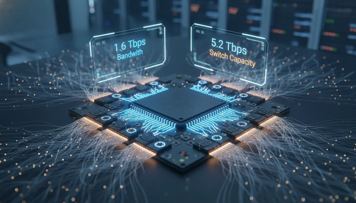
Every doubling of switch capacity — 12.8 Tbps, 25.6 Tbps, 51.2 Tbps, now 102.4 Tbps coming — has doubled the bit rate per electrical lane (SerDes). At 224 Gbps PAM4, a copper trace on a printed circuit board can carry data only a few inches before signal integrity collapses. The industry has been masking this with retimers, DSP-heavy pluggable optical transceivers, and aggressive forward error correction, but the energy and latency costs keep climbing. A single 51.2 Tbps switch loaded with 64 ports of 800G pluggable optics burns roughly 2,000 watts just in pluggables — about a third of the entire switch power budget — and adds a copper-to-optical-to-copper conversion on every link.
CPO eliminates that round trip. Instead of running a 224 Gbps electrical signal across the board to a faceplate cage, the switch ASIC talks to a silicon photonics engine sitting millimeters away inside the same package. Fiber, not copper, leaves the package. The result is a 3–4x reduction in interconnect energy (from roughly 15 pJ/bit on a 51.2T pluggable system down to under 5 pJ/bit on CPO), substantially better signal integrity, and a clear scaling path to 1.6T per port and beyond.
"We used to argue about which generation of pluggable optics could keep up with the next switch ASIC. By 2026 the only honest answer is — none of them. The next switch is built around the photonics, not the other way around."
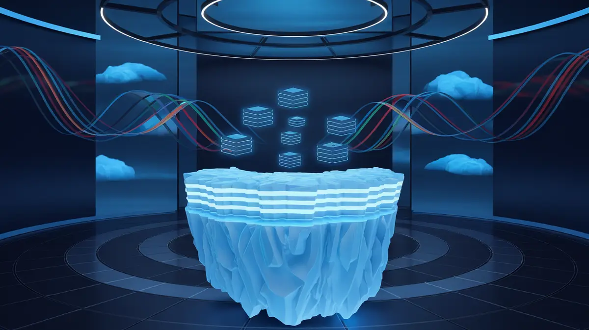
What Actually Sits on the Package
A CPO module is not one chip but a small ecosystem of co-designed silicon: a network or GPU ASIC, one or more silicon photonics engines, an external laser source (ELS) piped in via fiber, and a fiber array unit (FAU) that brings dozens to hundreds of single-mode fibers off the package. Four building blocks define the design.
Micro-Ring Modulators
Wavelength-selective silicon resonators that imprint data onto a CW laser at sub-picojoule energy per bit. Compact enough to put eight or sixteen on a single die — the foundation for dense WDM and the heart of NVIDIA Quantum-X Photonics.
External Laser Sources (ELS)
Continuous-wave lasers from Coherent, Lumentum, Sumitomo, and II-VI live outside the package — easier to cool, easier to replace, and decoupled from the ASIC thermal envelope. CW-WDM multi-wavelength combs are the 2026 standard.
TSMC COUPE Packaging
TSMC's Compact Universal Photonic Engine integrates photonics into the same SoIC/CoWoS-S flow that builds AI accelerators. NVIDIA Quantum-X Photonics is built on COUPE; Broadcom and Marvell are not far behind.
Fiber Array Units
Hundreds of single-mode fibers pigtailed to the package edge with sub-micron alignment. Yield, repair, and serviceability of the FAU is the unglamorous engineering problem that decides whether CPO actually scales.
Who Is Shipping CPO in 2026
| Vendor / Product | Capacity | Where It Wins |
|---|---|---|
| NVIDIA Quantum-X Photonics & Spectrum-X Photonics | 115.2 Tbps switch, 144 ports of 800G | The first hyperscale CPO design announced for production AI clusters. Built on TSMC COUPE, paired with Quantum-3 InfiniBand and Spectrum-X Ethernet for million-GPU AI factories. |
| Broadcom Bailly / Tomahawk 5 CPO | 51.2 Tbps now, 102.4 Tbps next gen | The merchant-silicon path. Broadcom's CPO Tomahawk drops into Microsoft, Meta, and Oracle networks without any ecosystem lock-in. Tomahawk 6 CPO at 102.4T is sampling in 2026. |
| Marvell 3D Silicon Photonics | 1.6T optical engine, 6.4T per package | 3D-stacked photonics integrated under a custom XPU. Targeting hyperscalers building their own AI silicon — AWS Trainium, Microsoft Maia, Meta MTIA — and shipping under the Marvell COLOR initiative. |
| Lightmatter Passage | 256 Tbps photonic interposer | A wafer-scale photonic interposer that any chiplet can sit on. Lightmatter has moved from photonic compute (Envise) into photonic interconnect, where the near-term revenue is. |
| Ayar Labs TeraPHY + SuperNova | 8 Tbps per optical chiplet | Optical I/O as a UCIe-compatible chiplet. Backed by NVIDIA, Intel, GlobalFoundries, and Lockheed. The cleanest model for retrofitting existing accelerator designs with optical egress. |
| Celestial AI Photonic Fabric | Memory-class optical interconnect | Optical fabric purpose-built for disaggregated HBM and accelerator memory pooling — the photonic complement to CXL in the AI rack. |
CPO vs Linear Pluggable Optics: The Transitional Fight
CPO is not the only answer to copper's wall. A faster-to-market middle ground called Linear Pluggable Optics (LPO) — and its near-cousin Linear Receive Optics (LRO) — removes the power-hungry DSP from the pluggable transceiver and runs the SerDes signal "linearly" out to the optics. LPO ships in volume today, cuts about 50 percent of the pluggable's DSP power, and requires no new packaging technology. Hyperscalers are buying LPO in 2025–2026 as a bridge while CPO ramps. By 2027–2028, the consensus across NVIDIA, Broadcom, and the OIF is that scale-up domains (NVLink/GPU-to-GPU) go to CPO first, while scale-out (rack-to-rack Ethernet/InfiniBand) follows once reliability, repair, and yield catch up.
The Hard Problems Nobody Has Fully Solved
CPO's economics are beautiful in a slide; its engineering is not. Three open issues define the field in 2026.
Field repair. A pluggable transceiver fails, a technician swaps it in 90 seconds. A CPO module fails, the whole switch line card or — worst case — the whole optical engine has to come out. The reliability bar for CPO is therefore an order of magnitude higher than for pluggables, and the supply-chain pressure on optical OSATs (ASE, Amkor, SPIL) is intense.
Laser sourcing. The CW lasers that feed the photonics engine remain the single most failure-prone component. Putting them outside the package (the ELS architecture) is the now-standard answer, but it pushes complexity onto fiber routing and connector counts. Coherent's CW-WDM laser shipments doubled in 2025 and will roughly double again in 2026 — a quiet supply story behind the entire CPO ramp.
Yield, test, and burn-in. A 51.2 Tbps CPO switch has dozens of micro-rings, hundreds of fibers, and tens of thousands of solder connections that must all pass at wafer test before the part is worth shipping. The industry is still climbing the learning curve TSMC, Foxconn-SPIL, and ASE built for 2.5D HBM packaging — only now with photonics in the loop.
What CPO Means for AI Buyers in 2026
- Million-GPU clusters become physically feasible. CPO is the single technology that closes the bandwidth-vs-power gap separating today's 100,000-GPU AI factories from the next decade's million-GPU buildouts at OpenAI Stargate, xAI Colossus 2, and the Microsoft–OpenAI supercomputers.
- Network power drops sharply. Eliminating four to five copper-to-optical conversions per link cuts interconnect power 3–4x at the link level and ~30% at the cluster level — direct savings against the data center power crisis.
- Latency falls. Removing pluggable DSPs and electrical retimers shaves nanoseconds per hop — enough to materially improve all-reduce and all-to-all collectives over NCCL and RCCL, where every microsecond compounds across thousands of GPUs.
- The roadmap is now optical-first. Vendor 2027–2028 plans (NVIDIA Rubin Ultra NVLink, Broadcom Tomahawk 7, Marvell next-gen XPUs) treat copper as a stub between the die and the on-package optical engine.
- Supply, not silicon, is the gating constraint. CW lasers, fiber arrays, and TSMC COUPE capacity are all sold out into 2027. Procurement timelines for any production CPO deployment now stretch 12–18 months.
Where Photonics Goes Next
The same physics that made CPO inevitable inside the switch will eventually push optics down into the package edge of the accelerator itself — optical I/O on the GPU. Ayar Labs and Lightmatter are already shipping that picture; NVIDIA's own published roadmap implies it for the Rubin-Ultra-and-beyond generation. Further out, thin-film lithium niobate (TFLN) modulators promise 5–10x lower modulation energy than today's silicon designs, hollow-core fiber from Corning and Lumenisity offers a 30 percent latency reduction over conventional single-mode fiber, and photonic interposers from Lightmatter and Celestial AI start to dissolve the line between "compute fabric" and "network fabric" entirely.
The deeper story is that AI training and inference have become an exercise in moving data, not just multiplying it. The chip costs $30,000. The cluster costs a billion. The grid struggles to feed it. The single piece of physics that decides whether the next AI factory can be built at all is no longer transistor scaling — it is the energy and bandwidth of moving a bit. In 2026, that bit, more and more often, is a photon.