HBM4 and the AI Memory Wall: How High-Bandwidth Memory Is the Real Bottleneck of Generative AI in 2026
- Internet Pros Team
- May 13, 2026
- AI & Technology
For most of the last decade, the conversation about AI hardware was a conversation about compute — how many FLOPS, how many TOPS, how many transistors NVIDIA could squeeze onto a single die. In 2026, that conversation has quietly changed. Every frontier model — GPT-5, Claude Opus 4.7, Gemini 3, Llama 5, DeepSeek-V4 — is now bottlenecked not by arithmetic but by memory bandwidth. The chip can multiply faster than the DRAM can deliver weights, and the cost of an idle math unit waiting on data is the dominant inefficiency in modern AI. That problem has a name — the memory wall — and its 2026 answer is a new generation of High-Bandwidth Memory called HBM4, now shipping in volume from SK Hynix, Samsung, and Micron, and stacked onto every flagship AI accelerator that matters.
Why Memory, Not Compute, Now Defines AI Performance
A modern transformer in inference mode does something deceptively simple: it reads a giant pile of weights from memory, multiplies them by a small activation vector, and writes the result back. For a 70-billion-parameter model running at 8-bit precision, that is roughly 70 GB of data moved per token. A high-end NVIDIA Blackwell GPU can do tens of trillions of multiply-accumulate operations per second — but if the memory subsystem can only feed it a few terabytes per second, the math units sit idle most of the time. The result, measured on real production workloads, is utilization that often falls below 30 percent. The compute is there; the bandwidth is not.
This is the practical definition of the memory wall in 2026: the gap between how fast accelerators can compute and how fast their memory can deliver the data to compute on. Closing that gap is now the single highest-leverage investment in AI hardware, and HBM4 is the industry's answer.
"The model is already on the silicon. The question we lose sleep over is whether the bytes can get to the math fast enough. HBM4 is the first generation where the answer is — for now — yes."
What Actually Changes With HBM4
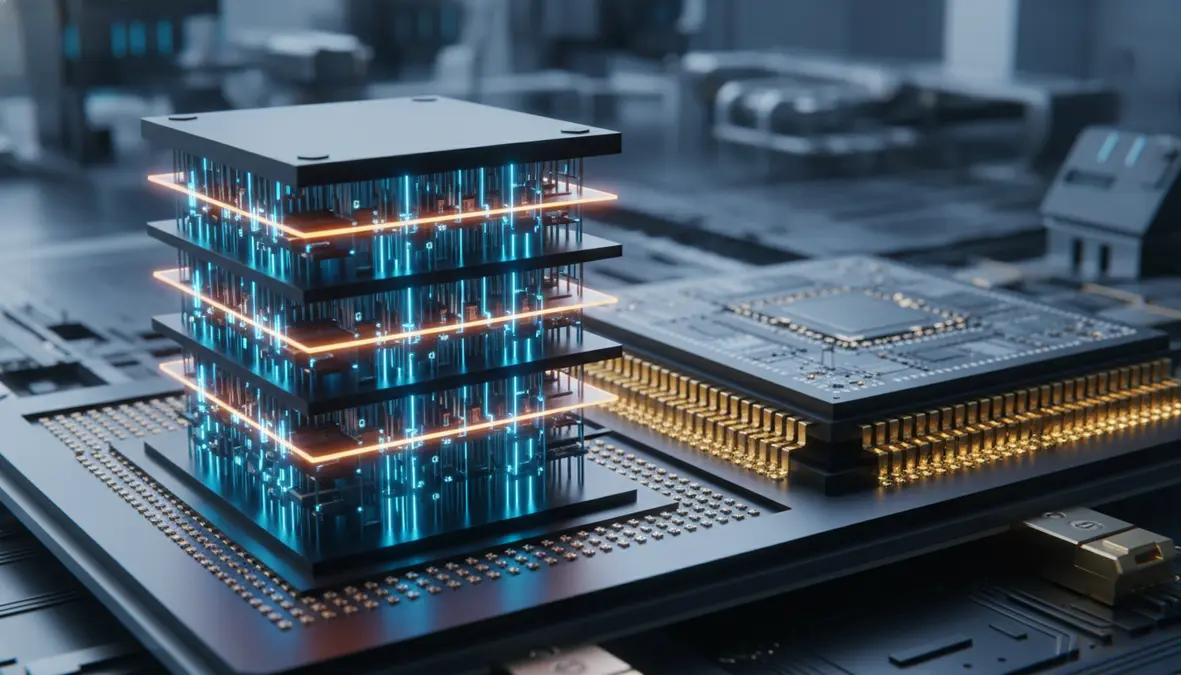
HBM4 is the fourth major generation of the JEDEC High-Bandwidth Memory standard. Like its predecessors, it stacks DRAM dies vertically and connects them with thousands of through-silicon vias (TSVs), sitting next to the accelerator die on a silicon interposer. What changes in HBM4 is the dial position on nearly every axis that matters.
2048-Bit Interface
HBM4 doubles the I/O width per stack from 1024 to 2048 bits. At equivalent pin speeds, that single change delivers twice the bandwidth — roughly 2 TB/s per stack — and is the foundational lever behind every HBM4 performance claim.
Hybrid Copper Bonding
Replacing solder microbumps with direct copper-to-copper bonding cuts stack height, slashes thermal resistance, and lets vendors push 16-high stacks reliably for the first time — the prerequisite for the 36–48 GB capacities AI workloads demand.
Customizable Base Die
For the first time, the logic die underneath the DRAM stack can be customized for individual customers. NVIDIA, AMD, and the hyperscalers can now embed their own controllers, prefetch logic, and even compute units beneath the memory.
Capacity Per Stack
HBM4 lands at 36 GB per stack at launch and a 48 GB variant on the roadmap. Pair eight stacks around a single GPU and a flagship accelerator carries 288–384 GB of HBM — enough to host a Llama-class model entirely on chip.
The Three Vendors Defining the 2026 HBM4 Market
| Vendor | Process & Packaging | Where They Win |
|---|---|---|
| SK Hynix | 1b-nm DRAM, MR-MUF molded underfill, advanced hybrid bonding pilot lines, exclusive primary supplier to NVIDIA Rubin | Volume leadership and the inside track on the highest-priced AI sockets. SK Hynix shipped first HBM4 samples in 2024 and is the reference supplier for NVIDIA's Rubin family. |
| Samsung | 1c-nm DRAM with EUV, full hybrid copper bonding line at Hwaseong, custom base die foundry capability through Samsung Foundry | Vertical integration. Samsung is the only HBM vendor that can also fabricate a customer's custom base die in-house — a structural advantage as hyperscalers demand silicon co-design. |
| Micron | 1-gamma DRAM, Boise and Taichung HBM4 lines, deep U.S. CHIPS Act subsidy support | The Western second source. Micron's HBM4 ramps a quarter behind Korea but is the default choice for U.S. national-security and supply-chain-diversification AI deployments. |
Who Is Buying HBM4 in 2026
The HBM4 customer list is short, concentrated, and almost entirely AI-driven. NVIDIA's Rubin platform, succeeding Blackwell, is built around eight HBM4 stacks per GPU and is the single largest HBM4 buyer. AMD's Instinct MI400 series targets the same socket with up to 432 GB of HBM4 per accelerator. Google TPU v7, AWS Trainium 3, Microsoft Maia 200, and Meta MTIA 3 all integrate HBM4 directly. Even the inference-specialist startups — Cerebras, Tenstorrent, d-Matrix, SambaNova — are increasingly designing HBM4 into their roadmaps, abandoning the old assumption that purpose-built inference silicon could rely on cheaper LPDDR or GDDR alternatives.
The economics tell the story. A single HBM4 stack at launch costs more than the entire mainstream PC DDR5 ecosystem priced per gigabyte. Yet hyperscalers buy them by the millions because the ratio of tokens-per-dollar at the system level is dramatically better than the alternative. When the accelerator costs $30,000 and is starved by memory bandwidth, paying another $5,000 in HBM to bring utilization from 30 percent to 80 percent is the most obvious optimization in computing.
The Hidden Constraint: Packaging
HBM4 cannot be soldered onto a motherboard. It must sit on a silicon interposer next to the accelerator, in a process broadly called 2.5D packaging. TSMC's CoWoS-L and CoWoS-S are the dominant variants; Intel's EMIB and Samsung's I-Cube are the alternatives. The capacity constraint on the entire AI industry in 2026 is not actually wafer starts in Taiwan or Korea — it is CoWoS packaging capacity. TSMC has tripled its CoWoS output two years running and is still rationing it to NVIDIA, AMD, and the hyperscalers. Until packaging catches up, HBM4 will remain the most allocated, most fought-over component in the AI supply chain.
What HBM4 Means for AI Buyers in 2026
- Larger models stay resident. A 384 GB HBM4 accelerator can host an entire 200B-parameter model in HBM, eliminating the offload-to-CPU memory hops that crushed prior-generation inference latency.
- KV-cache becomes cheap. Reasoning models, long-context agents, and RAG pipelines that depend on huge key-value caches finally fit comfortably on a single accelerator, transforming the unit economics of test-time compute.
- Inference tokens-per-second jumps step-function. Memory-bound workloads on Rubin and MI400 see 2x-3x throughput uplifts over Blackwell and MI300 — purely from bandwidth, before any architectural improvement.
- Custom base dies arrive. Hyperscalers can now ship accelerators with co-designed memory controllers, opening a new axis of competition that is invisible at the public datasheet level.
- Supply, not silicon, is the gating constraint. Order books for 2026–2027 HBM4 are full; new AI buildouts must lock allocation 12-18 months in advance.
Where the Memory Wall Goes Next
HBM4 is not the end of the story. The JEDEC roadmap already maps HBM4E with higher pin speeds and 16+ Gbps signaling, and HBM5, expected around 2028, is widely rumored to introduce processing-in-memory (PIM) primitives that move parts of the matrix-multiply workload onto the memory die itself — collapsing the memory wall from the other side. Samsung's HBM-PIM and SK Hynix's AiM are the precursors. If those technologies become standard, the boundary between compute and memory blurs in a way that the von Neumann architecture has not seen in seventy years.
For now, HBM4 is the single piece of silicon doing the most to keep the AI industry's growth curve intact. The training cluster, the inference fleet, the on-prem appliance, the sovereign-AI national initiative — they all run on the same scarce commodity, stacked in vertical layers of DRAM bonded with copper, sitting millimeters from the most expensive math units humanity has ever built. The story of AI in 2026 is, more than anything else, the story of how fast the memory can keep up.