Spintronics and MRAM in 2026: How Everspin, TSMC, Samsung, and Intel Are Building Magnetic Memory That Never Forgets and Barely Sips Power
- Internet Pros Team
- July 4, 2026
- AI & Technology
Every chip you own quietly fights the same battle: fast memory forgets everything the instant the power drops, and memory that remembers is painfully slow. Your processor keeps its working data in SRAM and DRAM because they are fast, but both go blank when powered off. Your phone keeps your photos in flash because it remembers, but flash is slow to write and wears out. For decades engineers accepted that you cannot have both. In 2026 a technology called MRAM - built on the physics of spintronics - is finally erasing that trade-off in real, shipping silicon: memory that is fast, remembers with the power completely off, and sips a fraction of the energy.
What Spintronics Actually Is
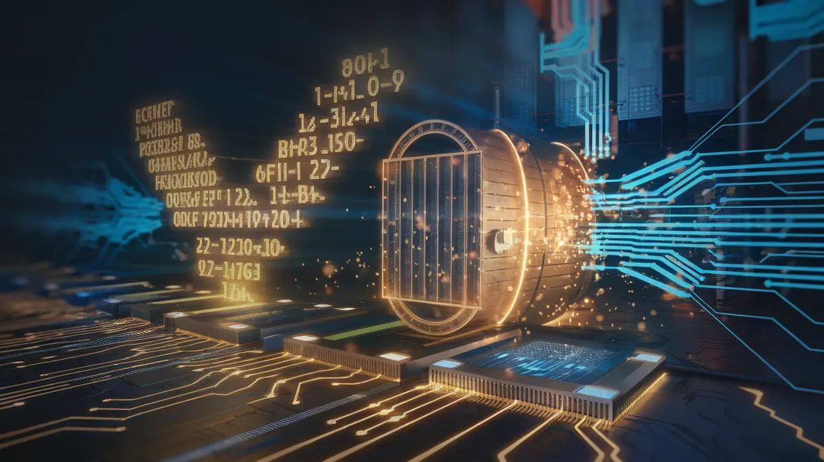
Ordinary electronics stores and moves information using the charge of electrons - counting how many are trapped somewhere to represent a 1 or a 0. Spintronics uses a second, quantum property every electron carries in addition to its charge: spin, which behaves like a tiny built-in magnet that can point either "up" or "down." Because spin is a magnetic state, it survives when the power is removed - a magnet does not forget which way it points. Encoding data in spin instead of charge is what makes non-volatile, low-power memory physically possible, and magnetoresistive RAM (MRAM) is the first spintronic device to reach mass production.
The Magnetic Tunnel Junction: One Bit, Two Magnets
At the heart of every MRAM cell sits a magnetic tunnel junction (MTJ) - a nanoscale sandwich of two magnetic layers separated by an insulating barrier just a few atoms thick. One layer is fixed, its magnetism locked in one direction. The other is free, and its direction can be flipped. When both layers point the same way, electrons tunnel through the barrier easily and the cell has low resistance (read as a 0). When they point opposite ways, resistance is high (read as a 1). This difference is called tunnel magnetoresistance, and reading a bit is simply measuring which resistance state the junction is in.
STT-MRAM
Spin-transfer torque MRAM flips the free layer by pushing a spin-polarized current straight through the junction. It is the dense, mature design shipping today - compact enough to replace embedded flash - but writing runs current through the fragile tunnel barrier, which limits speed and endurance.
SOT-MRAM
Spin-orbit torque MRAM adds a separate write line beside the junction, so the flipping current never crosses the barrier. That makes writes far faster and nearly unlimited in endurance - fast enough to challenge SRAM as on-chip cache - at the cost of a larger, less dense cell.
"For fifty years memory forced a choice: fast and forgetful, or persistent and slow. MRAM is the first technology to sit in the middle and mean it - it writes near working-memory speed, holds data for years with zero power, and does not wear out the way flash does. That is not a better flash. It is a new point on the map."
Why MRAM Matters Now
The reason MRAM has moved from lab to fab in 2026 is a practical one: as chips shrink to the most advanced nodes, the old embedded flash used to store a microcontroller's firmware simply stops scaling - it needs high voltages and extra process steps that modern logic cannot cheaply provide. MRAM slots in as a drop-in embedded flash replacement (eMRAM) that scales with the logic around it, boots instantly, and survives heat far better - which is why automotive and industrial chips adopted it first. At the other end, engineers are eyeing MRAM to replace power-hungry SRAM caches, enabling normally-off computing: a device that cuts power to idle blocks entirely and resumes instantly, because the memory never lost its state. For battery-powered IoT sensors and edge-AI devices that spend most of their life asleep, that is transformative.
MRAM vs. the Memory You Already Know
| Property | SRAM | DRAM | NAND Flash | MRAM |
|---|---|---|---|---|
| Keeps data with power off | No | No | Yes | Yes |
| Write speed | Fastest | Fast | Slow | Fast |
| Endurance (write cycles) | Unlimited | Unlimited | Limited | Very high |
| Density / cost per bit | Low / high | High / low | Highest / lowest | Medium |
| Standby power | Leaks | Refresh needed | None | None |
The takeaway is not that MRAM wins every row - it is that MRAM is the only column that never answers "No" to keeping data without power while still writing quickly. It will not out-cheap NAND for bulk storage or out-pack DRAM for main memory. Its sweet spot is everywhere persistence, speed, endurance, and low idle power all matter at once.
Who Is Building the Industry
What began as physics-prize research is now a manufacturing race across the biggest names in chips:
- Everspin Technologies - the pioneer and first to ship commercial MRAM, supplying discrete STT-MRAM and persistent memory for industrial, automotive, and data-center use.
- TSMC - offers embedded MRAM as a production option on its advanced nodes, letting fabless customers put non-volatile memory directly on their logic chips.
- Samsung - ships embedded MRAM in volume and is pushing MRAM research toward in-memory computing and cache-class speeds.
- Intel & GlobalFoundries - both qualified embedded MRAM on their process lines, with GlobalFoundries' 22FDX eMRAM widely used in microcontrollers and IoT parts.
- SK Hynix, TDK & Renesas - advancing MRAM for standalone memory, read/write heads, and microcontrollers, while research labs race SOT-MRAM toward the cache.
The Honest Trade-Offs
MRAM is real and shipping, but the engineers scaling it are candid about the hard parts:
- Density lags. An MTJ cell is larger than a DRAM or flash cell, so MRAM cannot yet match them on raw capacity or cost per bit - it targets embedded and specialty roles, not bulk storage.
- Writing still costs energy. Flipping a magnet with current takes more write energy than the best charge-based cells, and STT designs stress the thin tunnel barrier over time.
- Manufacturing is exotic. Depositing atom-thin magnetic stacks with uniform quality across a wafer is a specialized process that only a handful of fabs have qualified.
- Read margins are tight. The resistance gap between a 0 and a 1 is small, so sensing circuits must be precise, and stray magnetic fields have to be managed.
"You will not replace all the DRAM and flash in the world with MRAM tomorrow. It wins first exactly where the old memory is breaking - firmware on advanced nodes, always-on sensors, chips that must survive heat and boot instantly - and it spreads outward from there as density improves and cost comes down."
What This Means for Business
You do not have to design chips to feel the effects of non-volatile memory. MRAM is part of a broader shift toward hardware that is persistent by default and energy-frugal - devices that wake instantly, keep their state through power loss, and run for years on a coin cell. That reshapes what is possible in the products every business relies on: smarter IoT sensors that survive on tiny batteries, industrial and automotive systems that boot the moment they are needed, and edge-AI devices that keep learned data on-chip without draining power. The near-term move is not to chase a memory type by name, but to recognize that the same relentless demand from AI and connected devices that is reshaping processors is now reaching memory too - and to ask your hardware and platform partners how instant-on, low-power, non-volatile designs could make your products more reliable and longer-lived.
At Internet Pros, we help businesses make sense of fast-moving technology and turn it into a practical roadmap - from strategy to the software and automation that tie new systems together. Get in touch to talk through what emerging technology could mean for your operation, or explore more technology insights on our blog.