Glass Core Substrates in 2026: How Intel, Samsung, SKC Absolics, and LG Innotek Are Replacing Organic Packaging to Unlock Bigger, Faster AI Chips
- Internet Pros Team
- June 13, 2026
- AI & Technology
Every headline about artificial intelligence celebrates the silicon - the GPUs, the chiplets, the transistors shrinking toward atomic scale. But the unglamorous slab the chip is mounted on, the package substrate, has quietly become one of the biggest bottlenecks in computing. For decades that substrate has been made of organic resin, and as AI accelerators grow into sprawling assemblies of GPU dies and high-bandwidth memory stacks, that organic material is literally bending under the strain. The fix arriving in 2026 sounds almost too simple: build the substrate out of glass. From Intel's research fab in Arizona to Samsung, SKC's Absolics plant in Georgia, LG Innotek, and glassmakers Corning, AGC, and Schott, the industry is racing to replace warping organic packages with flat, stable, high-density glass core substrates - and it could reshape how every advanced chip is built.
What a Substrate Actually Does - And Why It Matters
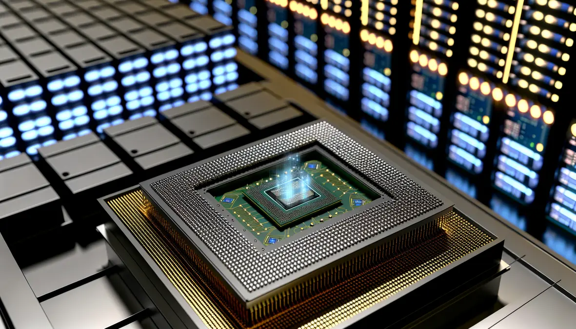
A processor die cannot connect to a circuit board directly. Its connection points are far too small and far too numerous. The package substrate sits in between: a multi-layer board with thousands of tiny wires that fan the die's dense signals out to the larger pads of the motherboard, while delivering power and carrying high-speed data. Today's high-end substrates are built from Ajinomoto Build-up Film (ABF) - an organic resin layered over a fiberglass core. It is cheap, mature, and has served the industry well.
The problem is scale. A modern AI accelerator is no longer a single chip; it is a system-in-package stitching together compute chiplets and multiple HBM memory stacks, sometimes spanning an area several times the old reticle limit. Organic substrates that big warp - they bow and ripple under heat and mechanical stress, breaking the delicate solder connections and capping how large and dense a package can get. The material that got us here cannot take us where AI needs to go.
Organic (ABF) Substrate
Resin over a fiberglass core. Cheap and proven, but warps at large sizes and limits how fine and dense the wiring can be.
Glass Core Substrate
A rigid glass core in place of resin. Exceptionally flat and dimensionally stable, enabling far larger packages and tighter interconnects.
Through-Glass Via (TGV)
A laser-drilled, metal-filled hole that carries signals and power straight through the glass - the vertical highway of the package.
"The package has become the new circuit board, and the circuit board has become the new bottleneck. Glass changes the math entirely - a substrate that stays perfectly flat at twice the size lets you put more compute and more memory next to each other than organic resin ever could. This is one of the most important materials shifts in advanced packaging in twenty years."
Why Glass Wins
Glass is not a novelty here - it is a genuinely better engineering material for the job. Its advantages stack up in exactly the dimensions that matter for AI-class packages:
- Extreme flatness and stability. Glass barely expands with heat and resists warping, so packages can grow far larger - vendors point to roughly 50% bigger body sizes - without the connections cracking. Flatter panels also mean higher manufacturing yield.
- Much finer interconnects. The smooth, rigid surface lets foundries pattern far tighter wiring, supporting on the order of 10x the routing density of organic substrates - critical for feeding bandwidth-hungry chiplets and HBM.
- Cleaner high-speed signals. Glass has excellent electrical properties (a low loss tangent), so high-frequency data and power move with less distortion - a natural fit for co-packaged optics and next-generation memory.
- Through-glass vias. Lasers can drill clean vertical channels through glass, enabling dense, direct paths for signal and power that organic cores struggle to match.
Who Is Building It
| Player | Role in the Glass Substrate Race |
|---|---|
| Intel | An early and vocal champion, with a dedicated glass-substrate research line in Arizona and a stated goal of bringing the technology to high-volume products in the second half of the decade. |
| Samsung & LG Innotek | Korean giants racing to industrialize glass packaging - Samsung Electro-Mechanics (SEMCO) and display affiliates, alongside LG Innotek, are building pilot lines and targeting customer samples. |
| SKC / Absolics | SKC's subsidiary Absolics built a US glass-substrate plant in Covington, Georgia - backed by CHIPS Act funding and partnered with Applied Materials - aiming to be a first mover in commercial supply. |
| Corning, AGC & Schott | The specialty glassmakers supplying the ultra-flat, high-purity glass cores the entire ecosystem depends on. |
The Hard Part: Glass Breaks
For all its promise, glass brings a thorny set of manufacturing problems that explain why this transition is measured in years, not months.
- Brittleness. Glass cracks and chips far more easily than resin. Handling thin glass panels through dozens of fab steps without breakage demands entirely new equipment and processes.
- Drilling clean vias. Cutting millions of precise, defect-free through-glass vias with lasers - without micro-cracks that propagate later - is among the toughest yield challenges.
- An immature supply chain. The tooling, materials, and know-how for high-volume glass packaging are still being built out, so early capacity is limited and costs are high.
- Metal-to-glass adhesion. Getting copper wiring to bond reliably to a smooth glass surface across thermal cycling is a materials-science problem in its own right.
What This Means for Business and IT Leaders
- Packaging is now a competitive battleground, not a commodity. The performance of next-generation AI servers will increasingly be decided by how chips are packaged, not just how transistors are printed. Glass is a leading indicator of who can build the biggest, fastest accelerators.
- Expect a gradual ramp, starting at the high end. Glass substrates will debut in flagship AI and data-center silicon where performance justifies the cost, then trickle toward the mainstream later this decade as yields improve.
- Watch the supply chain, not just the logo on the chip. Whether your hardware roadmap holds may hinge on glassmakers and packaging houses most buyers have never heard of. Supply concentration is a real risk to price and availability.
- It compounds other shifts you are already tracking. Glass cores pair naturally with chiplets, HBM, and co-packaged optics - the same trends driving the AI infrastructure buildout. Treat them as one connected story when planning capacity.
The Bottom Line
Glass core substrates are a textbook example of how progress in computing has shifted from the transistor to everything around it. As Moore's Law slows, the gains increasingly come from packaging - from how cleverly we wire many chips together into one system. Organic substrates carried the industry for thirty years, but they cannot stay flat at the sizes AI now demands. Glass can.
The transition will be slow, expensive, and full of yield headaches, and the first products will be premium data-center parts rather than the chip in your laptop. But the direction is set. The companies that master glass packaging - and the leaders who understand that the substrate, not just the silicon, now defines a chip's ceiling - will hold a quiet but decisive advantage in the race to build the machines that power artificial intelligence.