High-NA EUV Lithography in 2026: How ASML's TWINSCAN EXE:5200 Is Powering the Next Generation of AI Chips at Intel, TSMC, and Samsung
- Internet Pros Team
- May 21, 2026
- AI & Technology
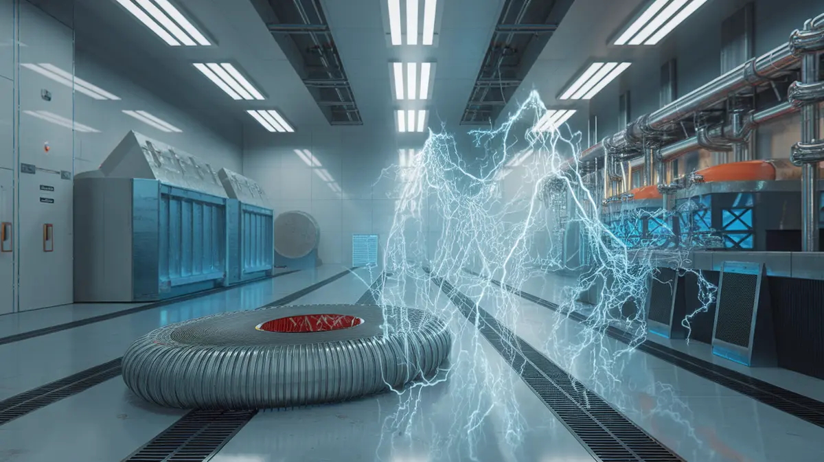
For the past decade, the entire AI revolution has been quietly riding on a single Dutch machine. ASML's TWINSCAN NXE series — the extreme ultraviolet (EUV) scanners that print every leading-edge chip from NVIDIA's Blackwell GPUs to Apple's M-series to Google's TPUs — has been the choke point of the modern compute economy. In 2026, that machine just got a successor. ASML's TWINSCAN EXE:5200, a $400-million-per-unit High-Numerical-Aperture (High-NA) EUV system with a 0.55 NA anamorphic optical column from Carl Zeiss SMT, has crossed from R&D into high-volume manufacturing. Intel's 14A, TSMC's A14, and Samsung's SF1.4 are the first three logic processes built around it, and the AI accelerator roadmaps from NVIDIA Rubin to AWS Trainium 3 are quietly recalibrating around what the new optics make possible.
Why High-NA EUV Was Inevitable
Standard EUV scanners — the 0.33-NA NXE:3800E generation now installed in roughly 250 fabs worldwide — top out at a resolution of about 13 nm half-pitch in a single exposure. To go finer, foundries have to double-pattern: print the same layer twice with carefully offset masks. Each extra pattern adds a mask set, an alignment error budget, two more etch steps, and roughly 30% to the wafer cost. By the 2nm logic node, the most aggressive layers were already triple- and quadruple-patterned, and the cost curve for the 1.4nm generation pointed straight up.
High-NA EUV exists to solve exactly that problem. Increasing the numerical aperture of the projection optics from 0.33 to 0.55 shrinks the diffraction-limited spot size, dropping single-exposure resolution to roughly 8 nm half-pitch. Layers that needed two EUV exposures at the previous node now need one. Mask count drops, cycle time drops, defectivity drops, and yield climbs — exactly what the industry needs to keep Moore's Law alive into the angstrom era.
"Every node from 14A forward is built around the EXE:5200. We are not negotiating slots — we are negotiating production weeks. The customer that loses one week of High-NA throughput loses an entire product generation."
The Tools and Players Inside Active Fabs in 2026
| Foundry / Node | High-NA EUV Status | What It Enables |
|---|---|---|
| Intel 14A / 10A | First commercial customer of the EXE:5000 (2024) and EXE:5200 (2026), with multiple systems running in D1X Oregon and Fab 52 Arizona. Pairs High-NA with RibbonFET gate-all-around transistors and PowerVia backside power delivery. | Intel Foundry's comeback bet. 14A targets a 15-20% performance-per-watt gain over 18A and is the process behind upcoming Falcon Shores and Clearwater Forest AI accelerators. |
| TSMC A14 / A16 | EXE:5200 systems installed at Fab 20 in Hsinchu Science Park, with high-volume production targeted for late 2026. A16 (1.6 nm) introduces Super Power Rail backside delivery; A14 is the first node to use High-NA broadly. | The default process node for NVIDIA Rubin, AMD MI400-series, Apple M6/A21, and most hyperscaler custom silicon entering production in 2027-2028. |
| Samsung SF1.4 | EXE:5200 deployments at S5 fab in Hwaseong and the new Pyeongtaek P4 line. Combined with second-generation MBCFET nanosheet transistors and SF2Z backside delivery. | Samsung Foundry's gambit to win back high-margin logic customers it has lost to TSMC. SF1.4 is the basis for Exynos 2600 and a planned Qualcomm dual-sourcing arrangement. |
| SK Hynix & Micron HBM4 / DRAM 1c | High-NA is now in qualification for the most aggressive DRAM cell layers on the 1c (sub-10 nm class) node, where the cost of multi-pattern DUV had become prohibitive. | HBM4 stacks at 16-Hi with up to 64 GB per stack — the memory bandwidth backbone of every 2027+ AI training accelerator. |
| IMEC / Albany Nanotech R&D | The pre-competitive R&D consortium running the 1.0 nm and beyond pathfinder lots, where the entire industry first sees how High-NA behaves with CFET, 2D channel materials, and forksheet transistors. | The reference platform that defines what shows up in commercial fabs three years later. The 1.0-nm "A10" roadmap currently being lit there is the 2029-2030 logic node. |
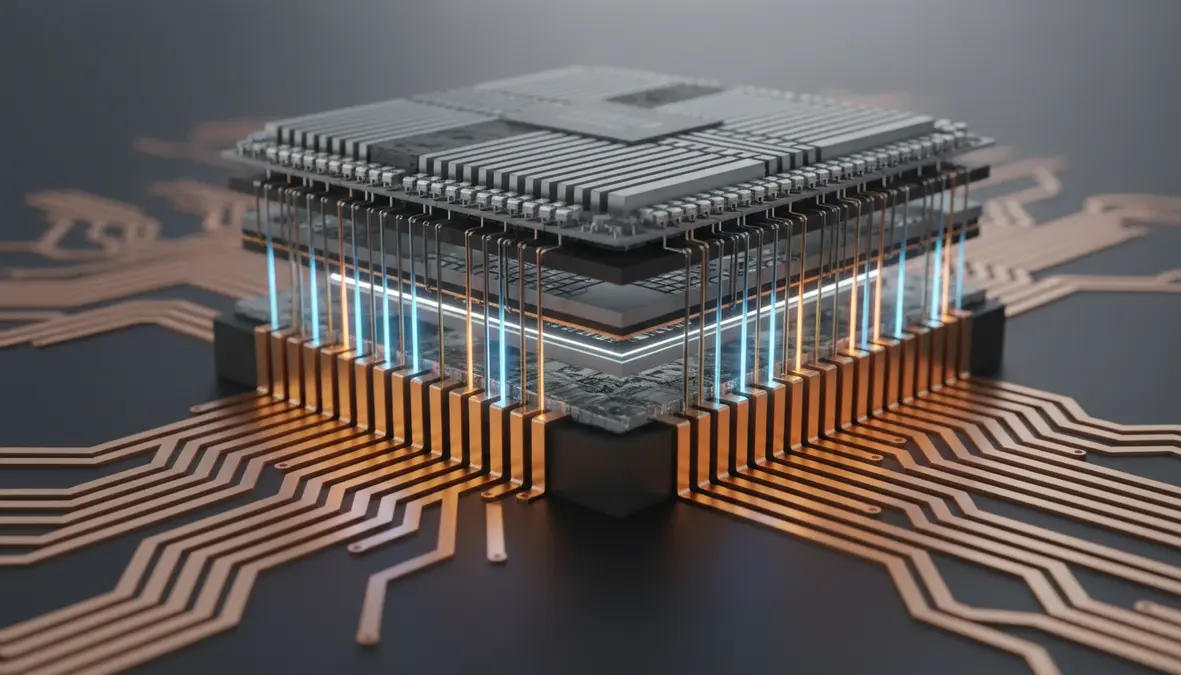
What's Different Inside the Machine
A High-NA EUV scanner is not just a faster version of its predecessor — it is a fundamentally re-architected optical system. Numerical aperture describes how strongly an optic can bend light; jumping from 0.33 to 0.55 required replacing every mirror in the projection box with larger, more steeply curved, and more precisely figured molybdenum-silicon multilayer reflectors. Zeiss SMT spent over a decade polishing the new mirrors to sub-angstrom flatness — the figuring tolerance is, by some measures, the most precise large-area surface ever manufactured.
Anamorphic Optics & Half-Field Stitching
At 0.55 NA the projection cone got so wide it no longer fit on a standard reticle. ASML's answer was an anamorphic design: 4x demagnification in one axis, 8x in the other. The cost is that each exposure now covers only half of the previous full field (26 × 16.5 mm). Designs that span a full die must be stitched from two half-field exposures — which puts new demands on overlay metrology and EDA tooling from Synopsys and Siemens.
A Heavier, Faster, Hungrier Stage
To hit a throughput of 195+ wafers per hour, the wafer stage accelerates at over 7 g while holding alignment to sub-nanometer precision. The tool weighs over 150 metric tons, draws roughly 1.4 MW, and ships to a customer in 13 separate cargo flights. A single EXE:5200 installation now takes a fab the better part of a year to qualify.
Resists, Pellicles, and Stochastics
Higher resolution means fewer EUV photons per printed feature, which amplifies stochastic defects — random missing or extra pixels caused by photon shot noise. The industry response has been metal-oxide resists from Inpria/Lam Research, dry resist processing, and a new generation of CNT-based pellicles from IBM and Mitsui Chemicals capable of surviving 600+ W EUV sources.
Computational Lithography Everywhere
Inverse lithography (ILT) and source-mask optimization (SMO) — once advanced extras — are now mandatory for every High-NA layer. ASML's Brion division, Synopsys Proteus, and Siemens Calibre run massive GPU clusters to pre-distort masks so the printed result matches the design. A High-NA mask now takes longer to compute than to write.
The Hard Problems That Remain
The supply chain is one company deep. ASML is the only manufacturer of EUV scanners on Earth, and Zeiss SMT is the only optics house that can build the mirrors. A single fire at the Zeiss facility in Oberkochen or the ASML campus in Veldhoven would halt the global leading edge. Governments now treat both sites as strategic infrastructure on par with semiconductor fabs themselves.
Mask infrastructure has not kept up. A High-NA mask blank is a six-inch quartz substrate coated with 40+ pairs of Mo/Si multilayer, capped with absorber, and inspected at actinic wavelength (13.5 nm). The world has fewer than a dozen actinic inspection tools, and the ramp from KLA and Lasertec is the silent bottleneck most outside the industry never see.
Cost-per-wafer has not yet inflected downward. The EXE:5200 list price is roughly twice the NXE:3800E, and a single exposure on it costs about $2.50 — versus $1.10 on the older tool. The economics only close once layer-doubling savings outweigh the per-exposure premium. The first commercial High-NA layers in 14A are still net-positive only because of the patterning steps they eliminate.
Export controls have hardened. The US BIS and the Dutch government have formally restricted EXE-class shipments to mainland China through at least 2027. SMIC and CXMT are responding with multi-patterned 0.33-NA EUV they can still buy, while research programs at Tsinghua and SMEE pursue a longer-shot steady-state microbunching (SSMB) alternative light source. The geopolitical fault line of the 2030s runs straight through this hardware.
What High-NA EUV Means for the AI & Hardware Industries
- AI chip roadmaps are now node-locked. NVIDIA Rubin, AMD MI400, AWS Trainium 3, Google TPU v7 Ironwood, and Microsoft Maia 200 are each tied to a specific High-NA process. Slipping a node means slipping an entire product generation; ordering capacity now is a strategic procurement decision, not an engineering one.
- The HBM4 cliff is real. Without High-NA in DRAM, the bandwidth-per-watt curve flattens before 2028. Every hyperscaler training-cluster roadmap assumes 16-Hi HBM4 stacks at the new node — and that assumption rests on EXE:5200 throughput at SK Hynix, Samsung, and Micron.
- EDA tooling becomes a moat again. Anamorphic stitching, ILT, and stochastic-aware OPC put Synopsys, Siemens EDA, and ASML Brion at the center of the design flow. The chipmakers that integrate computational lithography deepest into their PDKs will get yield ramps months earlier.
- Packaging eats some of the pressure. Not every chip needs the leading edge. Chiplets on TSMC CoWoS-L, Intel Foveros Direct, and Samsung X-Cube let designers use High-NA only on the dies that truly need it, keeping cost manageable.
- Sovereign chip strategies hinge on access. The CHIPS Act, EU Chips Act, Japan Rapidus, and Korea K-Chips Act all assume EXE-class machines on local soil by 2027. Without them, "sovereign foundry" is a marketing slogan, not a capability.
The Road to Hyper-NA and Beyond
ASML has already disclosed the next step. Hyper-NA EUV — a 0.75-NA projection system — is in active development at Zeiss SMT, with a first commercial tool targeted for the early 2030s. Beyond that, the roadmap diverges. The mainstream path runs through CFET (stacked complementary FETs) and eventually 2D-channel transistors built around molybdenum disulfide or tungsten diselenide — the post-silicon era IMEC has been quietly modeling for a decade. The exotic path bets on alternative light sources: SSMB, free-electron lasers, or even sub-10-nm EUV at 6.x nm.
For the next five years, however, the story is simpler. One Dutch company, one German optics house, and three or four customers willing to write a $400 million check per tool will continue to decide how fast the AI economy can scale. The EXE:5200 is the bottleneck that everyone — from hyperscalers buying GPUs to startups training frontier models — quietly depends on. In 2026, it finally moved from "promising lab tool" to "the machine that prints the future." The wafers have started rolling. Now the rest of the industry has to catch up.